- EasyCard
- Trade
- Help
- Announcement
- Academy
- SWIFT Code
- Iban Number
- Referral
- Customer Service
- Blog
- Creator
With the combination of CoWoS packaging and N2 technology, can TSMC maintain its position at the top of the global chip manufacturing process?


TSMC is currently the most advanced chip manufacturer in the world. With excellent process yield, clear development roadmap, and consistent and stable execution capabilities, TSMC has a leading advantage in the short, medium, and long term. The company plans to invest an additional $38 billion to $42 billion in capital expenditures in 2025, of which about 70% will be used for advanced process technology, 10-20% for advanced packaging, and the remaining 10-20% for special technology research and development. This series of layouts means that TSMC not only needs to consolidate its technological leadership position, but also further expand its production capacity to prepare for the growth of market demand in the coming years.
From the perspective of the proportion of revenue from various technologies, the importance of this high capital expenditure is obvious. Currently, cutting-edge processes account for 74% of the company’s total revenue, which shows the key role of advanced processes in TSMC’s future growth.
The launch of N2 and its competition with the Intel generation
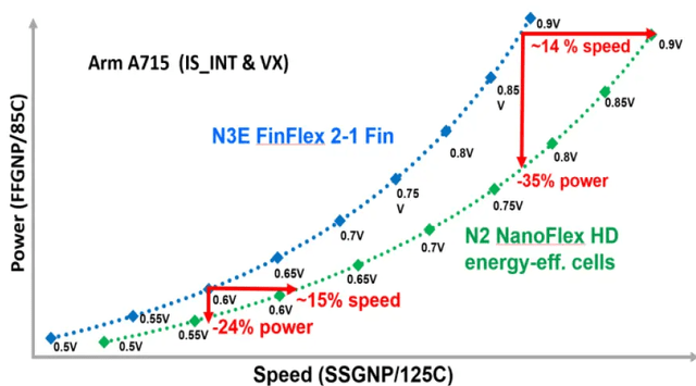
TSMC’s cutting-edge technology has always been the key to its revenue, and the 2nm (N2) process node that is about to enter mass production in the second half of 2025 will greatly affect TSMC’s future growth trajectory. Compared with N3E, the speed of N2 is expected to increase by 15% at the same power consumption, and if the same operating speed is maintained, the power consumption can be reduced by 24% -35%.
During TSMC’s latest earnings call, the CEO specifically mentioned N2 and its successor node A16. He emphasized that TSMC is still in a leading position in meeting the demand for high-performance computing, and almost all major innovators are collaborating with TSMC. It is predicted that with the promotion of 2nm in the fields of smartphones and high-performance computing (HPC), the number of tapeouts (officially entering the design stage before production) will surpass 3nm and 5nm in the first two years. N2 is still advancing according to plan, and mass production is expected in the second half of 2025, with a speed of capacity improvement similar to N3.
It is worth noting that TSMC’s close cooperation with customers such as Apple and NVIDIA has enabled it to maintain its industry-leading yield in advanced processes. Data shows that TSMC’s N3 process yield is as high as 84%, while Samsung’s yield is only between 50% and 60%. As for Intel 3, I have not found reliable yield data, but in terms of transistor density, it is closer to TSMC’s N5 than N3.
Currently, there are rumors that TSMC’s N2 yield has reached 60%, while Intel’s 18A is progressing slowly with a yield of only about 20% -30%. This is crucial for market competition, as the revenue share of advanced process nodes is constantly increasing. For example, it is said that TSMC’s N3 production capacity has been booked until 2026, and some N5 production capacity has even been adjusted to N3 to meet demand.
Based on historical data, TSMC’s 2nm is expected to bring considerable revenue within a year of mass production. Looking back at the past two years, revenue from 5nm and 3nm has grown rapidly, while nodes below 7nm remain stable. Therefore, even if N2 is launched, it will not have a significant impact on TSMC’s revenue from other advanced processes, but will promote overall growth.
Looking back at the past decade, TSMC has surpassed Intel in technology and officially surpassed them in revenue in 2022, leading the way ever since. Former Intel CEO Pat Kissinger once tried to catch up with TSMC through the “four-year, five-node” plan. Although the plan was not ultimately achieved on schedule, Intel still expects to mass produce the 18A process in the second half of 2025.
18A and N2 may be technically equivalent, but TSMC has more advantages in terms of production and capacity expansion. In addition, TSMC has rich experience in customer tapeout, while Intel’s foundry has not yet truly produced advanced process chips for external customers on a large scale. Even if 18A has technological leadership, Intel may still be limited by production capacity, while TSMC can rely on the stable cash flow brought by N5 and N3 to support the rapid increase in N2 production capacity.
If we speculate on the future revenue contribution of N2 based on data, the monthly production capacity target for the end of 2025 is 50,000 wafers, which will increase to 125,000 wafers by the end of 2026. Assuming linear growth in production capacity, approximately 1 million wafers will be produced throughout 2026.
Market rumors suggest that the price of N2 wafers is around $30,000. Based on this calculation, N2 may bring in $30 billion in revenue in 2026, accounting for 22.5% of the annual revenue. In contrast, N3 contributed 20% of the revenue after five quarters of mass production, and N2 is expected to surpass this achievement.
Advanced packaging and CoWoS capacity expansion
In addition to advanced processes, TSMC’s advanced packaging technology is also an important growth engine, especially CoWoS technology. Against the backdrop of explosive AI demand, CoWoS is in short supply, especially for packaging capacity of AI accelerators such as NVIDIA H100 and B100.
Currently, TSMC’s CoWoS production capacity is still limited, resulting in some orders needing to wait in line for several months. To address this issue, TSMC plans to increase its CoWoS production capacity to 30,000 wafers per month by the end of 2024, an increase of about 150% from the end of 2023. This expansion plan can not only meet the demand for AI chips from customers such as NVIDIA, AMD, and Amazon, but also further consolidate TSMC’s dominant position in the high-performance computing market.
In addition, TSMC is accelerating the advancement of SoIC packaging technology, which can achieve chip stacking at different process nodes, improving performance and power efficiency. Apple may be one of the first major adopters of SoIC technology. In contrast, Samsung and Intel are still lagging behind in advanced packaging technology. Samsung’s 2.5D and 3D packaging solutions are still in the experimental stage, while Intel’s Foveros 3D stacking technology is currently limited to specific product lines.
With the continuous growth of AI computing demand, CoWoS and SoIC are expected to become one of TSMC’s important revenue growth points in the next few years. TSMC’s CFO also emphasized in the latest financial report conference call that the growth rate of advanced packaging business will be significantly faster than the overall semiconductor market, and the compound annual growth rate is expected to exceed 30% in the next few years.
Valuation and future prospects
Considering TSMC’s technological leadership, strong order demand, and expanding advanced packaging business, the market is optimistic about its future performance. By 2025, TSMC’s N2 and CoWoS capacity expansion will drive its overall revenue growth, and the continued outbreak of AI computing demand is expected to provide additional growth momentum.
From the perspective of valuation, TSMC’s current Price-To-Earnings Ratio is about 20-22 times, which is still within a reasonable range compared to Nvidia (P/E over 60) and AMD (P/E around 40). Considering TSMC’s potential for performance growth in the next two years, the current valuation is still attractive.
In addition, TSMC’s dividend yield is about 2%, which is relatively high in the semiconductor industry. Considering its stable cash flow and capital expenditure plans, future dividends are expected to further increase, providing additional returns for long-term investors.
Overall, TSMC’s layout in advanced processes, advanced packaging, and HPC/AI markets gives it the potential for sustained growth. Although there may be short-term market fluctuations, in the long run, TSMC remains one of the most competitive companies in the semiconductor industry and deserves investors’ attention.
If you are interested in entering the market, you may consider trading at traditional securities firms such as Interactive Brokers, Jiaxin, and Tiger, or at the new multi-asset trading wallet BiyaPay.
Among them, BiyaPay supports trading of US and Hong Kong stocks and digital currencies. Through it, you can quickly recharge digital currency, exchange it for US dollars or Hong Kong dollars, and then withdraw the funds to your personal bank account, making it convenient to invest in TSMC. With advantages such as fast arrival speed and unlimited transfer limit, it can help you seize market opportunities in critical moments, ensuring fund safety and liquidity needs.
This method can be said to be fast, with no limit on the amount, no deposit or withdrawal troubles, and can also keep track of the stock market trends at any time, which can bring you a safe and efficient investment experience.
Peer comparison: TSMC’s unique position
As the only pure wafer foundry giant in the world, TSMC’s position in advanced manufacturing is almost unparalleled. This also means that it is not easy to directly compare TSMC with other companies. Therefore, it is more meaningful to focus on companies that can compete with TSMC in technology, such as Intel, or companies that are similar to TSMC in industry Competitive Edge, such as NVIDIA and ASML.
From a valuation perspective, the numbers of Intel and TSMC are somewhat similar, but in other key factors, TSMC completely surpasses Intel. TSMC’s valuation is slightly higher than that of Nvidia and ASML, although it is close to Nvidia in most indicators, ASML is slightly inferior. Considering TSMC’s irreplaceability in the global market, TSMC may still be undervalued and may enjoy a higher Price-To-Earnings Ratio in the future, just like ASML and Nvidia, relying on its technological advantages. Although it is difficult to give accurate numbers, considering its steady growth, TSMC’s stock price may rise by 20% to 37% by 2026, breaking through the $20 mark.
This comparison further confirms the view of staying away from Intel. According to data from Seeking Alpha, TSMC’s gross profit margin is currently very healthy, leading its peers by 12%. This means that TSMC not only has a technological advantage, but also far exceeds its competitors in financial health.
Risk factors cannot be ignored
One challenge that TSMC needs to pay attention to is the ongoing difficulties of Intel’s foundries. Intel’s foundry business is still very important to the US government, but it is currently unclear how the US government can ensure the continued existence of cutting-edge chip manufacturing in the US. There have been rumors that TSMC may cooperate with Intel and even send engineers to help improve the capacity of Intel’s foundries. The current difficulties of Intel’s foundries also indicate that TSMC’s leadership position in advanced semiconductor production is unshakable.
The pressure from the US government is still increasing, requiring more investment to flow into the US semiconductor manufacturing industry. This will inevitably affect overall profitability, as increased capital expenditures will compress profit margins. Nevertheless, TSMC is still driving the progress of global semiconductor manufacturing with its strong capital expenditures and technological innovation.
Overall, there are reasons for TSMC’s high valuation. Its strong technology Competitive Edge and foundry 2.0 vision have made it indispensable in the global semiconductor industry. With N2 technology, TSMC will continue to grow in the coming years, and it is expected that N2 will bring it $30 billion in revenue by 2026. Despite facing certain risks, TSMC still maintains its leadership position in the advanced semiconductor field.
*This article is provided for general information purposes and does not constitute legal, tax or other professional advice from BiyaPay or its subsidiaries and its affiliates, and it is not intended as a substitute for obtaining advice from a financial advisor or any other professional.
We make no representations, warranties or warranties, express or implied, as to the accuracy, completeness or timeliness of the contents of this publication.


Contact Us
Company and Team
BiyaPay Products
Customer Services


is a broker-dealer registered with the U.S. Securities and Exchange Commission (SEC) (No.: 802-127417), member of the Financial Industry Regulatory Authority (FINRA) (CRD: 325027), member of the Securities Investor Protection Corporation (SIPC), and regulated by FINRA and SEC.
registered with the US Financial Crimes Enforcement Network (FinCEN), as a Money Services Business (MSB), registration number: 31000218637349, and regulated by FinCEN.
registered as Financial Service Provider (FSP number: FSP1007221) in New Zealand, and is a member of the Financial Dispute Resolution Scheme, a New Zealand independent dispute resolution service provider.